Electronics
Driving the Virtual Design of Photovoltaics and Organic Electronics
Materials Modeling for Electronics Innovation
Modeling and simulation provide unique opportunity to study the structural, mechanical, electronic, optical and thermodynamic properties of organic molecules and is used extensively to design the next breakthrough electronic devices based on these materials. Two such examples are research into perovskites and OLED materials.
BIOVIA Materials Studio supports the characterization and development of existing and novel materials for display including OLED, organic semiconductors and beyond.
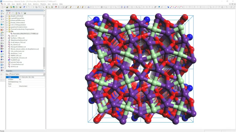
Perovskites as replacement for traditional silicon based photovoltaic cells promise more efficient conversion of light energy into electricity and significantly more flexible options for manufacture. However challenges remain in extending the lifetime of these materials, which are prone to degradation, and in replacing toxic components. OLEDs as light sources and as display technologies need developments in multiple areas to increase the efficiency, lifetime, and performance and reduce manufacturing costs. Development of blue emitter materials that allow for improved stability and efficiency, and methods to efficiently extract the light generated are two key challenges.
- OLEDs
- Photovoltaics & Perovskites
OLEDs
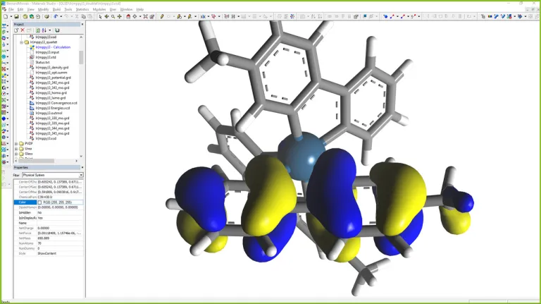
- Predict photo luminescence
- Predict Fluorescence and Phosphorescence
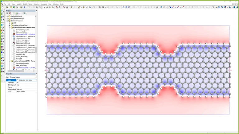
- Electron transport calculation using Green’s Function methods to monitor IV curve both for periodic and non-periodic structures
- Transmission function calculation at the interface
- Charge transport and carrier mobility in organic photo detectors
- Charge generation and charge separation process in bulk heterojunction
- Band offset and mobility calculation for metal impregnated metal sensors
- Polarizability and hyper polarizability for the organics adsorbed over active surfaces
- OLED or organic semiconductor’s structure confirmation using solid state NMR simulation
- Capability to design the full sandwiched model of electrode and organic device region
- Python-based high throughput automated workflows to calculate ground state and excited state properties to automatically generate a database
Photovoltaics & Perovskites
- Attachment of active layer with glass
- Simulate potential etching mechanisms
- Understand deposition, printing and adhesion to substrates
- Predict optical spectra using first principle calculations
- Predict solubility of materials in processing solvents using COSMOtherm
- Simulate curing of polymer films for encapsulation
- Predict hole migration and a recombination using ab initio MD
- Influence of molecular order on charge carrier mobility
Explore Our Methods
The world of product development is changing. Stay ahead of the competition with BIOVIA.
Join the conversation in the BIOVIA Materials Studio User Community!
Also Discover
Learn What BIOVIA Can Do for You
Speak with a BIOVIA expert to learn how our solutions enable seamless collaboration and sustainable innovation at organizations of every size.
Get Started
Courses and classes are available for students, academia, professionals and companies. Find the right BIOVIA training for you.
Get Help
Find information on software & hardware certification, software downloads, user documentation, support contact and services offering


